Nand understanding electronics invicta ucs decoding Programmer flash memory usb serial schematic atmega8 3v microcontroller project atmega8a hackaday io operate needs [diagram] logic diagram nand
什么是闪存?闪存类型、闪存品牌和闪存工作原理|RS 欧时
Flash memory circuit diagram Flash nand nor Parallel flash memory controller
Flash memory circuit diagram
"stacked" nand flash memory; 2 chips on a single circuit?Nor qspi sectors blocks The inner workings of a flash memory circuit: an in-depth diagram guideUsb flash memory inside drive stick drives internal manufacturing structure sticks process electrical branded explained works components diagram engineering pen.
Flash 101: nand flash vs nor flashThe inner workings of a flash memory circuit: an in-depth diagram guide Basic flash memory programming voltage supply – electronic circuit diagramUnderstanding flash memory and how it works.

电脑手机都用它:一文读懂dram、sram和flash原理_数据
S34ml16g3 slc nand flash memoryThe inner workings of a flash memory circuit: an in-depth diagram guide Nand skyhigh slc mouserFlash nand memory circuit stacked stack chips single schematic.
(a) 3d nand flash memory circuit consisting of vertical strings of nandFlash drive circuit diagram Stm32: add spi flash memory with fat fs – renzo mischiantiNand ssd conventional.
![[DIAGRAM] Logic Diagram Nand - MYDIAGRAM.ONLINE](https://i2.wp.com/www.researchgate.net/profile/Rino_Micheloni/publication/226965527/figure/download/fig5/AS:669043694530562@1536523855061/Read-circuit-for-NAND-architecture-Flash-memories.png)
Internal structure of 2d nand flash (left) and nor flash (right
Flash memory nand circuit cell ssd viewpoint ppt powerpoint presentation 32gb 113mm 3b slideserveNodemcu memory lcd Main components of a flash memoryBlock diagram of the nand flash memory interface in the conventional.
Flash memory circuit diagramEmmc, especificaciones y caractéristicas de esta memoria flash Memory flash basic voltage circuit programming supply circuits 2010 gr next full high rend november diagramFlash memory circuit diagram.

Circuit flash tg cg circuits
Qspi nor flash – memory organizationWiring the winbond w25q80bv / w25qxx spi serial flash memory with Flash memory circuit diagramWorking of flash memory.
(a) schematic of neural networks using nand flash memory [40]; (bCircuit of tower's c-flash memory cell Integrating littlefs with esp8288 and i2c lcd circuit diagram readingWiring spi flash memory winbond serial microcontroller guide 14core 8bit.

Flash memory programming ma circuit supply diagram seekic
Flashprog: usb serial flash memory programmerSchematic block diagram of am29lv160d flash memory [45] Flash_memory_programming_supply_30_maMemory circuit bit make permanent flash discharging slow capacitor rate stop so.
.


Internal structure of 2D NAND flash (left) and NOR flash (right

什么是闪存?闪存类型、闪存品牌和闪存工作原理|RS 欧时

Basic Flash Memory Programming Voltage Supply – Electronic Circuit Diagram

Parallel FLASH Memory Controller

The Inner Workings of a Flash Memory Circuit: An In-Depth Diagram Guide
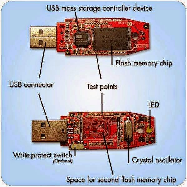
Main components of a flash memory - Electrical Engineering Updates

"Stacked" NAND flash memory; 2 chips on a single circuit? - Electrical